
Modern computing is nearing a physical wall. As artificial intelligence and high-performance data processing demand unprecedented computational power, traditional semiconductors—long the foundation of digital technology—are approaching their physical and architectural limits. The industry now faces a critical inflection point: finding what comes after the microchip.
This transformation is most visible at Nvidia, whose market value recently reached roughly $5 trillion, making it the world’s most valuable publicly traded company. Nvidia’s top-tier processors pack up to 208 billion transistors within a single chip, each unit priced around $30,000. These chips, when deployed by the thousands across data centers, form the computational backbone of modern AI infrastructure. Nvidia’s latest architectures are designed to function collectively, allowing multiple chips to operate as unified hyperscale systems rather than isolated processors.
However, as transistor density increases, the industry has hit limits dictated by physics. At the heart of chip manufacturing lies extreme ultraviolet lithography, a process driven by Dutch company ASML’s $380 million high-numerical-aperture system. This machine, often described as the “Extreme Machine,” projects light through photo masks to etch patterns onto silicon wafers. Yet even this technology cannot overcome the reticle limit—a fundamental boundary capping the size of a chip die at about 800 square millimeters. To achieve greater performance, manufacturers must combine multiple smaller chips, introducing complex interconnections and communication overheads that add both cost and design challenges.
In response, researchers are turning toward wafer-scale integration, an approach that abandons discrete chips altogether. Instead of cutting wafers into smaller dies, the entire silicon wafer serves as a single, monolithic processor. Palo Alto–based Cerebras has pioneered this model with its Wafer-Scale Engine 3 (WSE-3), a chip containing four trillion transistors and delivering 7,000 times the memory bandwidth of leading conventional processors. By embedding memory directly into the wafer, the WSE-3 reduces latency and condenses the computing footprint once reserved for entire data centers.
Tesla experimented with a similar concept in its Dojo project under Elon Musk before discontinuing it, though the architecture continues through ventures like DensityAI. Meanwhile, Lam Research, a major fabrication equipment supplier, has developed multi-column electron-beam lithography via its spinout Multibeam Corp. This technique may allow chipmakers to inscribe circuitry on larger wafers, circumventing the reticle constraint.
Together, these advances suggest that the microchip’s dominance may be waning. Wafer-scale integration and emerging lithographic techniques could usher in a new era of “data centers-in-a-box,” reshaping how computational infrastructure is built and redefining the limits of performance, scale, and efficiency that have governed digital technology for decades.
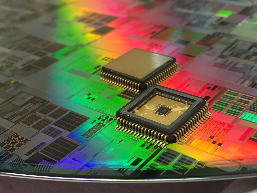
Featured image credits: Flickr
For more stories like it, click the +Follow button at the top of this page to follow us.